


 수량을 선택해주세요.


MSP430F149 개발보드
(MSP430F149 Board)
개요
- 본 제품은 MSP430F149 MCU를 탑재한 개발보드입니다.
- MSP430시리즈를 개발하거나 학습할때 사용하기 좋은 보드입니다.
특징
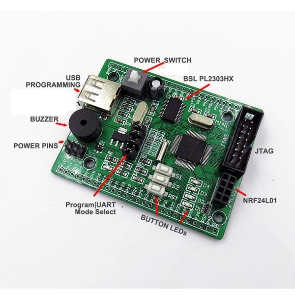
- Onboard USB BSL program download PL2303HX, you can download the program for itself or other board. High quality capactiors.
- Comes with 2 independent button input.
- Onboard manual reset button.
- Wireless NRF24L01 connector
- Comes with 4 test LEDs
- Buzzer circuit, can be used to play music
- Provide 32.768KHZ and 8MHZ two crystal connection
- Using standard JTAG interface (14-pin), support hardware simulation.
- All IO ports (including AD power, etc.) are led (not welded pin, can be up or down welding).
- Provide 3.3v and 5v output power supply pin.
- The board itself can be completed part of the experiment, also be directly inserted into the use of protoyping board, expand more features.
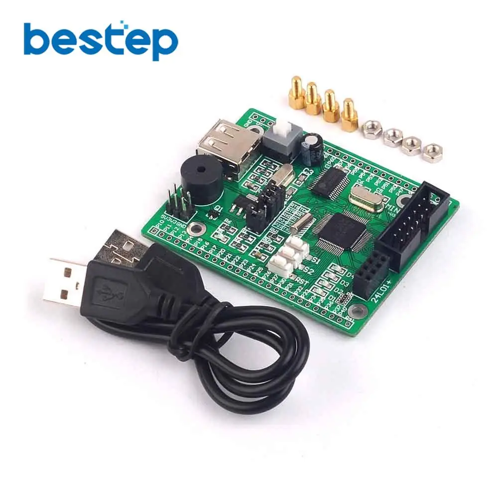
- Packages include:
- MSP430f149 (mini430) mini development board
- Male to Male extension cable
- 2 sets of copper pillars
문서
- flash tool
- Programming
- Use on board PL2303 USB-TTL programmer, and connect as follow:
RXD - P11 TXD - P22 RTS - TCK DTR - RST GND - GND
- Target board should also be powered independently.
- To use regularly, remove all the connection jumpers, and set
RXD - P34 TXD - P35
- To download programe, open software MSPFET, open download file, turn on board power, use "AUTO" to download
- Troubleshooting
- Erase failed. Synchronization error. - this is normally a wiring problem.
- Init failed. Could not open port. - check serial uart setttings, com port, baudarate, driver, etc.
-
Tutorial
IO Features
- MSP430 port has P1, P2, P3, P4, P5, P6, S and COM (different models, including the port is not only the same, such as MSP430X11X series only P1, P2 port, and MSP430X4XX series contains all the ports) Can be used directly for input / output.
- MSP430 system does not have special input / output instructions, input / output operations through the transfer instruction to achieve. Each bit of port P1`P6 can be used independently for input / output, that is, with bit addressing.
- Common keyboard interface can be directly used to simulate the port, with the query or interrupt control.
- As the MSP430 port only data port, no status port or control port, in practical applications, such as in the query input / output transmission, you can use a port or a few bits to send the status information, by querying the corresponding bit State to determine whether the peripheral is in the "ready" state.
Port function
- P1, P2 port: I / O, interrupt function, other on-chip peripheral functions such as timers, comparators;
- P3, P4P5P6 port: I / O, other on-chip peripheral functions such as SPI, UART mode, A / D conversion, etc .; (3) S, COM port: I / O, drive LCD.
- MSP430 ports have a wealth of control registers for users to achieve the appropriate operation.
- Where P1 and P2 have seven registers and P3 to P6 have four registers. By setting the register we can implement:
- each I / O bit is programmed independently;
- any combination of input, output and interrupt;
- P1, P2 All 8 bits can all be used as external interrupt handling;
- can be used so the instruction to register operation;
- can be byte input, output, can also be bit by bit operation.
- The functions of ports P1 and P2 can be implemented by their seven control registers. Here, Px stands for P1 or P2.
- PxDIR: input / output direction register. 8 bits are independent of each other, can be defined 8 pin input / output direction. 8 bits are reset after PUC. When using the input / output function, you should first define the direction of the port. As input can only be read, as output, readable and writable. 0: input mode; 1: output mode. Such as: P1DIR | = BIT4; //P1.4 output, P2DIR = 0XF0; // high 4-bit output, low 4-bit input.
- PXIN: input register, read-only register. The user can not write it, only by reading the contents of its register to know the I / O port input signal. So the direction of its pin to be selected as input. Such as re-keyboard keyboard scanning program often read the line or column line port register value to determine the case. For example: unsigned char key;
P1DIR & = ~ BIT4; //P1.4 input ... Key = P1IN & 0X10; // output port P1.4 value ...
- PXOUT: output register. This register is the output buffer register of the I / O port, and the contents of the output buffer are read regardless of the pin direction definition. Change the contents of the direction register, the contents of the output cache are not affected. Such as: PIOUT | = 0X01; //P1.0 output 1, PIOUT & = ~ 0X01; //P1.0 output 0.
- PXIFG: interrupt flag register. His 8 flags indicate whether the corresponding pin has an interrupt request pending. 0: no interrupt request, 1: interrupt request. The interrupt flag is PXIFG.0 ~ PXIFG.7. It should be noted that: PXIFG.0 ~ PXIFG.7 share an interrupt vector, for multi-source interrupt. When any of the events caused by the interruption of processing, PXIFG.0 ~ PXIFG.7 will not automatically reset, must be determined by the software which is the event, and the corresponding logo reset. In addition, the external interrupt event time must be maintained at no less than 1.5 times the MCLK time to ensure that the interrupt request is accepted and the corresponding interrupt flag bit is set.
- PXIES: Interrupt Trigger Edge Select Register. If a pin of the port is allowed to be interrupted, it is also necessary to define the interrupt trigger mode for this pin. 0: rising edge triggers the corresponding flag to be set, 1: falling edge triggers the corresponding flag to be set. Such as: MOV.B # 07H, & P1IES; p1 Low 3-bit falling edge triggers an interrupt.
- PXIE: Interrupt enable register. Each port of the PX port has a bit to control whether the pin is allowed to be interrupted. 0: disable interrupt, 1: enable interrupt. MOV.B # 0E0H, & P2IE; P2 high 3 bits are allowed to interrupt.
- PXSEL: Function selection register. P1, P2 two ports also have other on-chip peripherals function, these functions and external contact with the chip through the multiplexing P1, P2 pin way to achieve. PXSEL is used to select the I / O port function of the pin and the peripheral module function. 0: select pin for I / O port, 1: select pin for peripheral module function. Such as: P1SEL | = 0X10; //P1.4 for the peripheral module function.
- Ports P3, P4, P5, P6 no interrupt capability, the rest with the same PI, P2. Remove the three registers associated with the interrupt P1, P2 and the three registers, ports P3, P4, P5, P6 of the four registers (usage with P1, P2) were PXDIR, PXIN, PXOUT, PXSEL available to users.
- Ports COM and S, they achieve a direct interface with the LCD chip. COM is the common terminal of the liquid crystal chip, and S is the segment terminal of the liquid crystal chip. The LCD chip output can also be configured as a digital output port via software