


 수량을 선택해주세요.


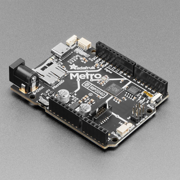
Metro RP2040 개발보드
(Adafruit Metro RP2040)
개요
- 본 제품은 Metro RP2040 개발보드 입니다.
- RP2040 칩을 장착한 아두이노 보드 폼팩터의 제품입니다.
- 3.3V 로직을 가지고 있습니다.
특징
- Choo! Choo! This is the RP2040 Metro Line, making all station stops at "Dual Cortex M0+ mountain", "264K RAM round-about" and "16 Megabytes of Flash town". This train is piled high with hardware that complements the Raspberry Pi RP2040 chip to make it an excellent development board for projects that want Arduino-shape-compatibility or just need the extra space and debugging ports.
- RP2040 main chip, 133MHz clock, 3.3V logic
- 16 MB of QSPI flash for program storage
- 24 GPIO, 4 of which are also analog inputs
- Micro SD card socket wired up for SPI interfacing, also has extra pins connected for advanced-user SDIO interfacing (note that there's no released usage code for SDIO in Arduino/Python, so this is a super-cutting-edge setup)
- Onboard RGB NeoPixel
- Onboard #13 LED
- Stemma QT port for I2C peripherals and sensors
- Reset and Boot buttons on PCB edge
- Pico Probe debug port - 3 pin JST SH compatible
- SWD debug port - 2x5 0.05" standard connector
- USB Type C power and data
- 5.5mm / 2.1mm DC jack for 6-12VDC power
- On/off switch for DC jack
- GPIO pin numbers match classic Arduino pins, other than A4/A5 which are D24 and D25 (there's only 4 ADC pins on the RP2040)
- RX / TX switch for swapping D0 and D1 locations
- You may be wondering about the RX-TX switch: we added this because traditional Arduino board start counting the GPIO for the digital pins with 0-7 and then 8-13. However, the D0/D1 pins are also traditionally the hardware UART Serial1, where D0 is Rx and D1 is Tx. On the RP2040, however, the UART pins are the other around: D0 is Tx and D1 is Rx. Thus a DPDT switch: flip one way to have the GPIO go in order of 0-7, flip the other way to have the logical locations of the hardware UART correct but now the pin order is 1, 0, 2, 3..7. Of course, it's also handy if, like us, you often swap the pins - now you don't need to require or cut/solder traces!
- Dual ARM Cortex-M0+ @ 133MHz
- 264kB on-chip SRAM in six independent banks
- Support for up to 16MB of off-chip Flash memory via dedicated QSPI bus
- DMA controller
- Fully-connected AHB crossbar
- Interpolator and integer divider peripherals
- On-chip programmable LDO to generate core voltage
- 2 on-chip PLLs to generate USB and core clocks
- 30 GPIO pins, 4 of which can be used as analog inputs
- Peripherals
- 2 UARTs
- 2 SPI controllers
- 2 I2C controllers
- 16 PWM channels
- USB 1.1 controller and PHY, with host and device support
- 8 PIO state machines
-