


 수량을 선택해주세요.


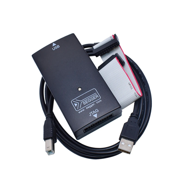
Segger J-link 디버거 프로그래머 V9
(J-link/Jlink V9 Debugger)
개요
- 본 제품은 Seggar사의 J-Link 디버거/프로그래머 V9클론 버전입니다.
- IAR EWARM, Keil MDK, Rowley CrossWorks, Atollic TrueSTUDIO, IAR EWRX, Renesas HEW, Renesas e2studio와 같은 메이저 개발환경에서 지원이 되는 프로그래머입니다.
- ARM 칩을 프로그래밍하고 디버깅하는데 사용됩니다.
- 디버거, USB 케이블, flat 리본 케이블 포함되어 있는 제품입니다.
- V9 버전으로 V8버전에 비해 빠른 속도와 안정성을 가지고 있습니다.
특징
-
Differences between JLink V8 and Jlink V9:
1. Different speeds :V8 supports up to 10M(JTAG debugging mode)/4M(SDW debugging mode), while Jlink V9 supports 20M (JTAG debugging mode)/ 15M (SDW debugging mode).
2, different stability :V9 driver IC has voltage adaptive ability, in the case of correct wiring, automatically adapt to the cpu voltage of the target board. All cpus from 1.8-5.5V can be debugged, while the V8 version can only debug 3.3v cpus, and the 5vcpu is very unstable.
3. JlinkV8 is easy to drop firmware and become a brick. I have a lot of V8s that are down and I have to rewrite the firmware, and the average user is left with a brick wall, which is basically not the case with V9.
4. Some of the latest cpuV8 models are no longer supported, while V9 supports almost all ARM cpus.
JLINK V9 Six features:
1. The main control chip adopts STM32F205, without losing the firmware.
2, can provide 3.3V voltage 0.8A current for the development board, 19 pin output 5V voltage, can adapt to 1.8V-5V voltage
3. Support standard JTAG interface and 2-wire SWD debugging interface. The speed can reach 20M(JTAG)/15M(SWD) per second.
4. Support debugging of all ARM chips, support MDK or IAR, and other standard JLink supported compilation environment IDE.
5, the original firmware, firmware automatic upgrade
문서
-
Instructions for Use (Must See) :
1, the simulator is completely in accordance with the original design, 1 foot 2 feet together can provide 3.3v output function (official marked as NC foot), the default shipment for the original does not output 3.3V, parents need power supply please open the shell (20PIN seat there break open without screws) switch jumper cap to 3V3 position (back interface diagram is still the official interface, please note!)
2. Due to the different power supply requirements of the target board, the driving ability of the simulator is limited. If the simulator is used to power the target board, it is easy to damage the simulator.
Port and indicator description:
1, Green, blinking at a frequency of 10Hz → simulator initialization.
2, Green, blinking → When the simulator is working, the indicator light will temporarily go out when an instruction is executed. Therefore, the blinking speed is determined by the interface speed of the target board. In low-speed interfaces, the indicator is off for a longer period than in high-speed interfaces.
3. Steady green → The emulator is initialized and in Idle state.
4, Green, 10ms→J-LINK heartbeat is extinguished every second. This function will be activated when the emulator is in Idle state for more than 7 seconds.
5, Orange → target board is in reset state.
6, Red, blinking at a frequency of 1Hz → The simulator has a serious error, which should not occur under normal conditions.
7. Plug in the target board and turn off the light → short circuit of the target board.
- http://www.segger.com/download_jlink.html