


 수량을 선택해주세요.


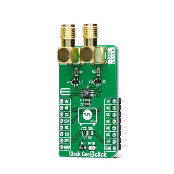
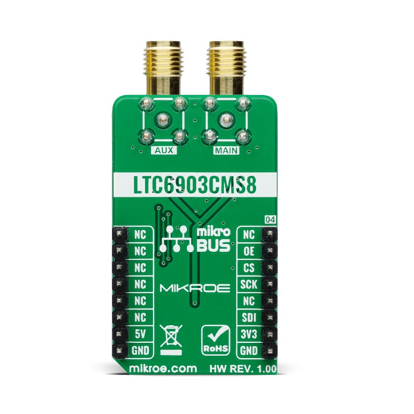
프로그래밍 가능 디지털 오실레이터 모듈 -LTC6903
(CLOCK GEN 5 CLICK)
개요
- 본 제품은 프로그래밍 가능 디지털 오실레이터 모듈 -LTC6903입니다.
- LTC6903 칩을 기반으로 디자인된 제품으로 1Khz에서 68Mhz의 주파수를 SPI 인터페이스를 통해 설정할 수 있습니다.
특징
-
Type Clock generator Applications Can be used for applications such as MCU clock source, clock source for a switched capacitor filter, or general replacement for a DAC/VCO combination On-board modules LTC6903 - a low-power self-contained digital frequency source providing a precision frequency from 1kHz to 68MHz set through a 3-wire digital interface from Analog Devices. Key Features Low power consumption, more reliable and vastly more versatile clocking solution, precision frequency from 1kHz to 68MHz, proprietary feedback loop, and more. Interface SPI Compatibility mikroBUS Click board size M (42.9 x 25.4 mm) Input Voltage 3.3V or 5V -
Clock Gen 5 Click is based on the LTC6903, a low-power self-contained digital frequency source providing a precision frequency from 1kHz to 68MHz set through a 3-wire digital interface from Analog Devices. The LTC6903 contains an internal feedback loop that controls a high-frequency square wave (VCO) operating between 34MHz and 68MHz. It is also a resistor controlled oscillator that offers an integrated serial resistor DAC and a set of digital frequency dividers. The oscillator frequency is inversely proportional to the resistance of the DAC, where step size ranges between 0.05% and 0.1% of the frequency.
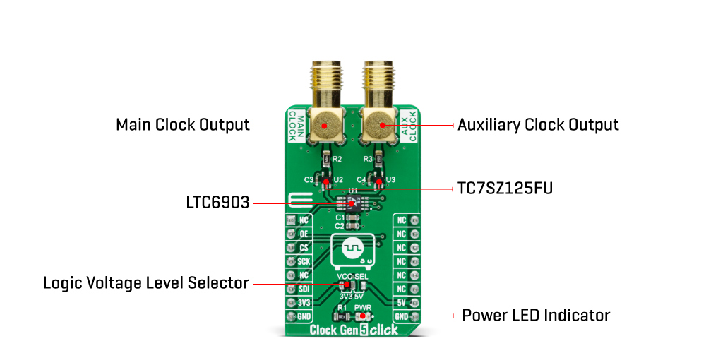
In the most frequency ranges, the output of the Clock Gen 5 Click is generated as a division of the higher internal clock frequency. This helps to minimize jitter and sub-harmonics at the output of the device. In the highest frequency ranges, the division ratio is reduced, which will result in greater cycle-to-cycle jitter as well as spurs at the internal sampling frequency. The output clock signals, available on the SMA connectors with an impedance of 50Ω labeled as MAIN and AUX CLOCK, before the output itself are primarily conducted through the TC7SZ125FU, a 3-state bus buffer allowing the LTC6903 to operate normally producing the required output.
Clock Gen 5 Click communicates with MCU using the 3-Wire SPI serial interface and operates at a clock frequency up to 20 MHz. The output signals are controlled by the output control bits MODE1 and MODE0, where the outputs can be disabled through these bits. When both output signals are disabled through the mode control bits, the internal oscillator is also disabled. The OE pin, routed on the RST pin of the mikroBUS™ socket, can also be used to asynchronously disable either output without shutting down the oscillator entirely.
This Click board™ is designed to operate with both 3.3V and 5V logic voltage levels selected via the VCC SEL jumper. It allows for both 3.3V and 5V capable MCUs to use the SPI communication lines properly. However, the Click board™ comes equipped with a library that contains functions and an example code that can be used, as a reference, for further development